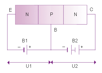
Figure 1. The common-base connection
|
Your name:
Your university:
Male/female? What is your background? |

The double-subscript notation is utilized in labeling terminal voltages, so that, for example, uBE symbolizes the increase in potential from emmittor (E) to base (B), whereas UBE symbolizes the potential between emmitor (E) and base (B). For reasons that will become apparent, currents and voltages commonly consist of superimposed DC and AC components (usually sinusoidal signals). The common-base (CB) connection is a two-port transistor arrangement in which the base shares a common point with the input and output terminals. The independent input variables are emitter current iE and the base-to-emitter voltage UEB. The corresponding independent output variables are collector current IC and base-to-collector voltage UCB. Practical CB transistor analysis is based on two experimentally determined sets of curves:

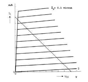
The common-emmittor (CE) connection is a two-port transistor arrangement in which the emittor shares a common point with the input and output terminals. The independent port input variables are base current IB and emittor-to-base voltage UBE, and the independent port output variables are collector current IC and emitter-to-collector voltage UCE. Like CB analysism CE analysis is based on:


The following constants are defined for DC currents:
The constant α is smaller than 1 and ß is mostly a value between 100 and 300.
Supply voltages and resitors bias a transistor; that is, they establish a specific set of DC terminals voltages and current, thus determining a point of active-mode operation (called the quiescent point or Q point). Usually, quiescent values are unchanged by the application of an AC signal to the circuit. With the universal bias arrangement only one DC power supply (Ucc) is needed to establish active-mode operation. Use of the Thevenin equivalent of the circuit (in figure 5) the resistor the AC current sees is a resitance RB and RB = R1*R2/(R1 + R2) and UBB = R1*Ucc/(R1 + R2). RB is the virtual input resistance.


If we neglect leakage current so that IEQ = (ß + 1)*IBQ and assume the emitter-to-base voltage UBEQ is constant (about 0.7 Volt), then we can represented IEQ = ICQ.
RL is the virtual resistance for the load. It is clear that IC = Ucc/RL - UCE/RL. The DC load line is a line as shown in figure 5 between the two points Ucc/RL and Ucc (source: McCraw-Hill Book Company). It is clear that amplifiers can be biased for operation at any point along the DC load line.
There is also a AC load line, but that line depends on the coupling capicitors C1, and C2 and the bypass capicitor CRE. The coupling capicitors confine DC quantities to the transistor and its bias circuitry. The bypass capicitors effectively remove the gain-reducing emitter resistor RE insofar as AC signals are concerned, while allowing RE to play its role in establishing ß-independent bias (gerichtheid). The capicitors are shorted in the circuit as it appears to AC signals. As RL(DC) = RC + RE so is RL(AC) = RC*RL(DC)/(RC + RL(DC)). Since RL(AC) is not equal to RL(DC) in general, the concept of an AC load line arises.
Enschede, Febr. 2004; updated: April, 28, 2004